Getting Started with PCB layout Editor
Setting up PCB Layout Editor
Open PCB Layout Editor
Select Imperial Icon on left Toolbar for Inches. Millimeters can be used if you prefer.
Both are in this guide. Inches first then Millimeters.
Research you PCB manufacturer requirements for board specifications
Example for https://docs.oshpark.com/design-tools/kicad/kicad-design-rules/
For OSHPark  2 layer boards service with Imperial units options:
Min trace clearance: 0.006 6 mil (0.1524mm) trace clearance
Min trace width: 0.006 6 mil (0.1524mm) trace width
Min via diameter: 0.020 20 mil (0.508mm) 5 mil (0.127mm) annular ring
(Corresponding to a 5 mil annular ring)
Min via drill diameter: 0.010 10 mil (0.254mm) drill size
Min via drill diameter: 0.005 5 mil (0.127mm) annular ring
Setting up Design Rules
Select Setup from the Top Menu bar then select Design Rules Select Global Design Rules Tab Enter Min track width: 0.006 (0.1524 mm) Enter Min via diameter: 0.020 (0.5080 mm) Enter Min via drill diameter: 0.010 (0.2540 mm) Add additional Tracks as seen in Figure 1 below. Track1 0.006 (0.1524 mm) Track2 0.008 (0.2032 mm) Track1 0.010 (0.2540 mm) Track1 0.012 (0.3048 mm) Track1 0.016 (0.4064 mm) Track1 0.020 (0.5080 mm)Figure 1
Setting up Boarder (Edge Cuts)
Set Grid: 10 mils(0.2540mm)
Select Edge Cut from the Layer Manager.
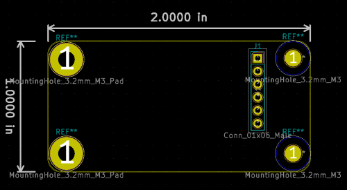
Select Place Tab on Top Toolbar then Select Dimension
Use this to measure the board size first. These dimensions can be deleted once Edge cut is complete.
Select from Right side tool bar Add Graphic Line
Draw lines to define you board Edge cut. When done change Select Front Copper F.Cu from the Layer Manager.
Adding Rounded Edges (Corners)
Select Edge Cut from the Layer Manager.
Select Add Graphic Art from Right Side Toolbar
Starting at top right corner. Count 10 dots back from each edge click one time with mouse.
Then move cross hair to edge of board click again and swing counter clock wise.
Repeat for each corner.
Now delete all four strait lines leaving only the 4 arc's.
Select Add Graphic Art from Right Side Toolbar and redraw the straight to each arc.
When done be sure to Select Front Copper F.Cu from the Layer Manager.
Drill Holes
Select Add Footprint from Right side Toolbar (IC Chip)
Type MountingHole_3.2mm (preferred choice)
Type MountingHole_3.2mm_M3_PAD (Copper ground)
Type SolderWirePad
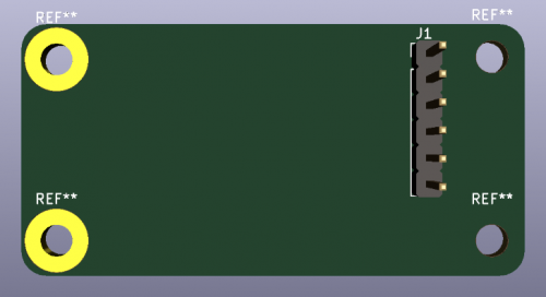
3D View
Select View Tab on Top Toolbar
Select 3D Viewer from drop down
Reading Netlist and placing footprints from components
Select Read Netlist from Upper Toolbar. Click on Read Current Netlist.
Click on components and move to place on board.
Now lets go to: ==Creating a component for KiCad Using SnapEDA == and add more components.

